I need to switch a 30Amp resistive DC load from a 5V microcontoller pin. This isn't PWM just occasional on/off.
I'm familiar with the design considerations for high speed switching - rapidly getting charge in and out of the gate to minimise time spent in the linear region but in this application I'm pretty sure I can safely simplify the design a great deal because it's only used as a discrete on/off control.
What I've come up with does seem uncomfortably slow so I thought I'd ask around in case I'm missing something!

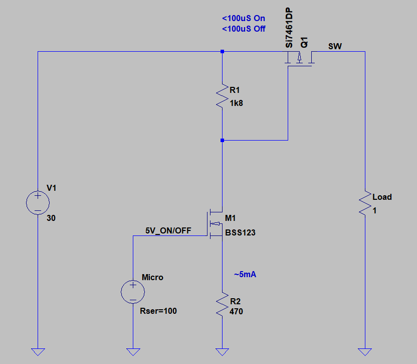
Q1 would actually be IPD50P04P413ATMA1 a 12mOhm P-Channel MOSFET, 50 A, 40 V. The total gate charge is less than 50nC so charging/discharging at around 5mA should take no more than 50nS x 1/0.005 = 10uS
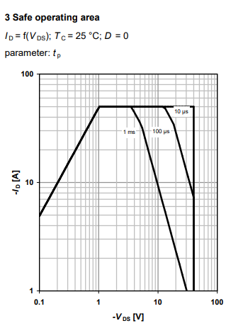
This keeps it in the top right corner of the safe operating area:

The DC input could be as high as 30V so to limit the gate voltage low swing, the 470R source resistor makes M1 act like a constant current sink (its threshold being around 2.5V). R1 maintains around 10V across it until the supply drops below 12V
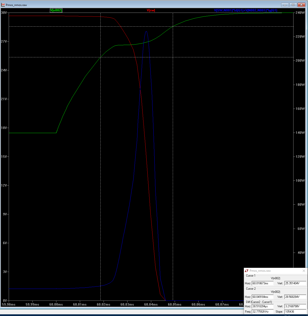
LTspice sim of ~30uS switch-off for part with even higher gate charge (120nC) seems OK:

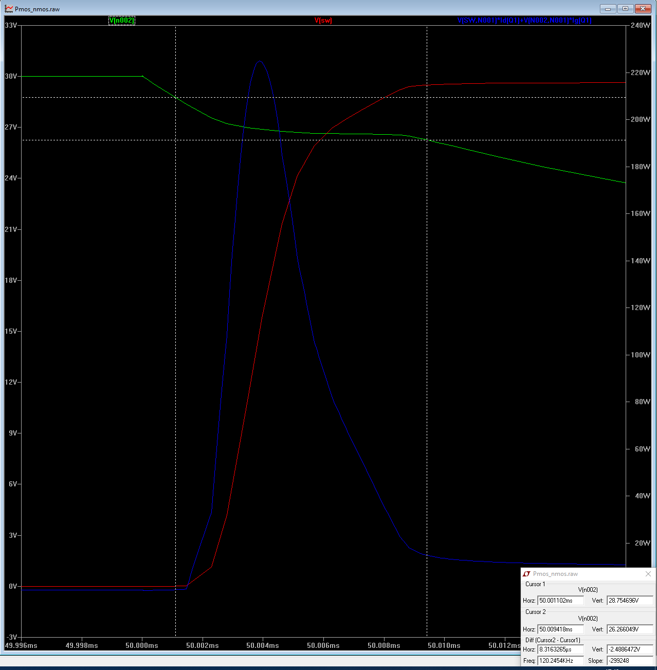
Green is gate voltage, red ouptut voltage and blue power dissipation in Mosfet. Switch-on should be a bit sharper and it is at <10uS:

Too good to be true? I'm so used to the pitfalls of Power PWM design that this simple application has me jittery
I'm familiar with the design considerations for high speed switching - rapidly getting charge in and out of the gate to minimise time spent in the linear region but in this application I'm pretty sure I can safely simplify the design a great deal because it's only used as a discrete on/off control.
What I've come up with does seem uncomfortably slow so I thought I'd ask around in case I'm missing something!
Q1 would actually be IPD50P04P413ATMA1 a 12mOhm P-Channel MOSFET, 50 A, 40 V. The total gate charge is less than 50nC so charging/discharging at around 5mA should take no more than 50nS x 1/0.005 = 10uS
This keeps it in the top right corner of the safe operating area:
The DC input could be as high as 30V so to limit the gate voltage low swing, the 470R source resistor makes M1 act like a constant current sink (its threshold being around 2.5V). R1 maintains around 10V across it until the supply drops below 12V
LTspice sim of ~30uS switch-off for part with even higher gate charge (120nC) seems OK:
Green is gate voltage, red ouptut voltage and blue power dissipation in Mosfet. Switch-on should be a bit sharper and it is at <10uS:
Too good to be true? I'm so used to the pitfalls of Power PWM design that this simple application has me jittery


Comment