
Re: Plasma Y-MAIN board LJ92-01200A
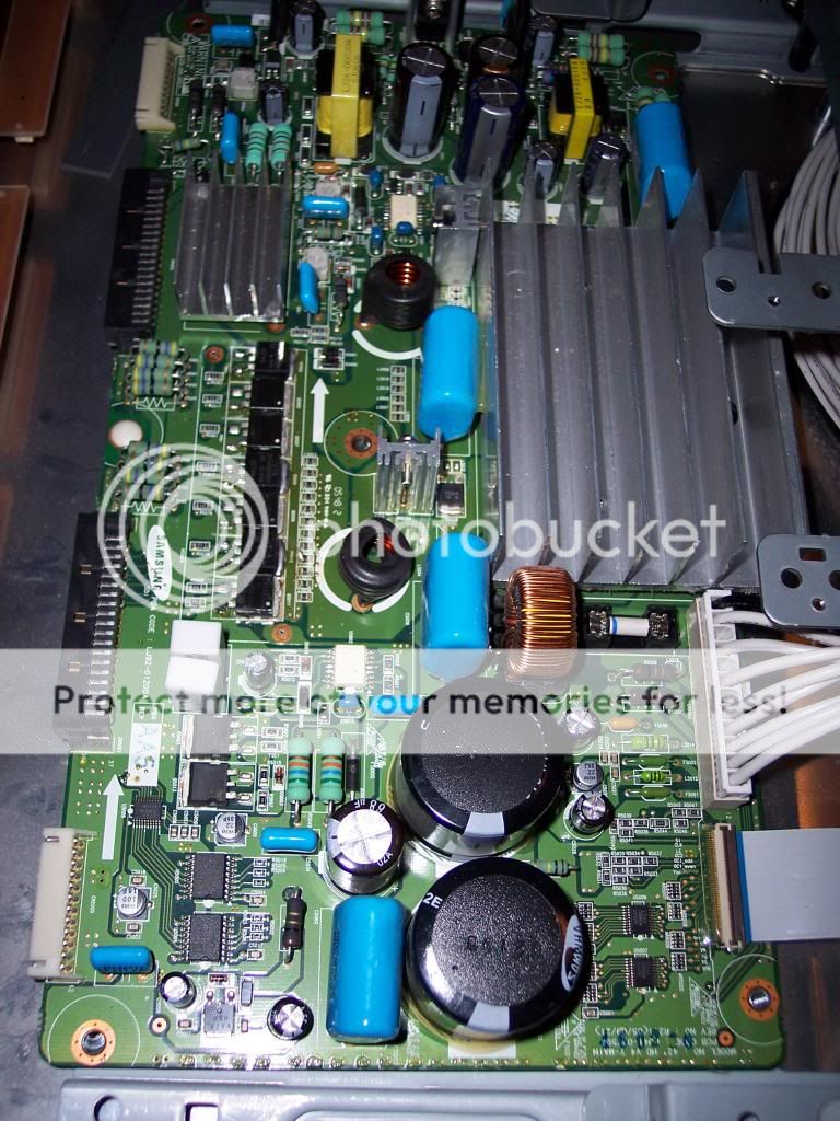
i was wondering if you guys had the diagram of the capacitors for this board Y-MAIN board LJ92-01200A...
i need C5052
and C5040...
-
Re: Plasma Y-MAIN board LJ92-01200A
I'm sure there's a rational explanation for that, lol. I would check the voltages on theymain against what's printed on the panel. Or could be xmain trouble as well.
You need an expert opinion so I'll just bow out now.Leave a comment:
-
Re: Plasma Y-MAIN board LJ92-01200A
Please see the attached image. I replaced the faulty diodes, resistors and mofset. I'm trying to run the TV with only the upper buffer board and this is what I get. (See picture) any ideas?Attached FilesLeave a comment:
-
-
Re: Plasma Y-MAIN board LJ92-01200A
Sorry I can't help you, my TV was disassembled and disposed of being I ran out of help and know-how.
Good luck.Leave a comment:
-
Re: Plasma Y-MAIN board LJ92-01200A
Hello,
I'm sorry to resurect an old thread but I'm trying to fix my TV and came across this.
The TV originally had sound but no picture.
I replaced the IPM (althou it wasn't blown as it turned out) and one of the blown mofsets.
The buffer boards are not shorted at this point althou I'm positive the lower one was the culprit as one IC is visibly burned out.
At this point I'm getting a reddish distorted picture with lower part of the low buffer visibly blown.
I checked the diodes and the resistors as specified in the thread and both resistors are burned as well as both D5018 and D5009 diodes. I was able to cross reference the markings on the D5018 but cannot find anything on the D5009 (says K7 79 on it) I have a K7 59 on a parts board that I could use. Can someone tell me if that would work or what the right specs are. Also the resistors are both 1ohm in paralel so .5ohms. Is it ok if I substitute them with one .5 ohm?
Thanks in advance.
AdamLeave a comment:
-
Re: Plasma Y-MAIN board LJ92-01200A
Anyone have any idea what I should check next ?
Thanks.Leave a comment:
-
Re: Plasma Y-MAIN board LJ92-01200A
Any ideas what to check next. Thought I was doing good =\Leave a comment:
-
Re: Plasma Y-MAIN board LJ92-01200A
OK, yes, that makes sense, it is for the control/logic board.
Since the voltages disappear if that is connected, I expect you still have a fault on your Y-main.Leave a comment:
-
-
Re: Plasma Y-MAIN board LJ92-01200A
Where does the small ribbon cable go?Leave a comment:
-
Re: Plasma Y-MAIN board LJ92-01200A
I get 194.5 at the black wire in the power connector on the y-sus for a brief moment and then it goes away once the TV clicks to standby.
If I do not plug in the small ribbon cable below the power connector on the Y-sus, it will stay on and read 194
Whats next ? =)Leave a comment:
-
Re: Plasma Y-MAIN board LJ92-01200A
Do you have VS reaching the Y-main board?Leave a comment:
-
Re: Plasma Y-MAIN board LJ92-01200A
Got my 3 new mosfets installed. Didn't do too bad getting them straight and flat.
Plugged the board into the TV with no buffers.
It still clicks on, then off and the green LED flashes.
I don't appear to have any shorts across either of the 2 black connectors. I checked the few hot pins vs all the ground pins on each connector.
I did notice that my new mosfets measure O.L. from the Gate to Source and from Gate to Drain. The existing mosfets measured about 14M ohms Gate to Drain and 2-5M ohms from Gate to Source.
The New and Existing mosfets all measured about 6.37M ohms Drain to Source. None of them make the meter beep though when on diode check mode for ohms.
So, what do I need to check next ?Leave a comment:
-
Re: Plasma Y-MAIN board LJ92-01200A
It's not a good idea to run the board without certain parts unless you're sure no damage will occur.Leave a comment:
-
Re: Plasma Y-MAIN board LJ92-01200A
Once I remove this 3rd, bad mosfet, can I plug the board in to see if it will "not" trip the tv into standby, or is that going to harm something else with out the mosfets attached ?Leave a comment:
-
Re: Plasma Y-MAIN board LJ92-01200A
Got all the paste cleaned up.
I then retested to double check...
I have one mosfet that reads 1.3 ohms between Gate and Source
It reads 100.1 ohms between Gate and Drain
It reads 99.2 ohms between Drain and Source.
Does this one need replaced too ?Leave a comment:
-
-
Re: Plasma Y-MAIN board LJ92-01200A
Hi,
pretty good question! I´ve read and learned alot from reading different posts in this excellent forum. I take my hat off to all the plasma and lcd gurus here! Great job and thanks!
I myself have abt 30 years of experience with crt tv´s, now getting familiar with lcd´s, but plasmas are still a book of seven seals to me. This one stood in my garage for abt 3 years, not knowing if it is worth the time to look for. Anyway, with the help of this forum i gave it a try and let´s see what happens.
While you are waiting for the mosfets maybe you can prepare the heatsinks for remounting. Same here, the thermal compound is as hard as a stone, no way to get it off with alcohol or something like that. I used a sharp scalpel to scratch it off. Worked fine for me but be careful not to make any deep scratches into the surface of the heatsinks. Did the same with the residue on the mosfets.
Did you encounter any probs with your buffer boards? I could locate one defective driver ic on the upper y-buffer board after removing those little heatsinks on them. The defective one had a little hole on its surface and after removing it from the pcb the resistance between supply rail and ground measured good.Leave a comment:


-
 Hello, I am looking for help to replace a damaged diode. The tristar was replaced and a diode was damaged in the process. I have a picture of the diode but dont have an exact donor. I mostly have macbooks for donors and only a few ipad and iphone boards. Diode part number: DSF01S30SCAP
Im not sure where to find the ipad board number. Anybody have an idea where else this diode is used on other boards? Thanks.... -
 Hello everyone, I'm repairing an LG TV backlight and I noticed some strange behavior when I touching the backlight strip with a missing Zener diode.
So I replaced the leds on the strips and they seemingly working fine, but soon as I touch the strip which has a missing Zener diode the whole backlight turns off for a few seconds and then turns back on.
Is this caused by the missing diode? If so what kind of zener diode should I use to replace it?.
The led strips has 9 6V leds.
-
 Hello everybody☺️ I am glad to be here and looking forward to a good discussion.
First of all, I am new here. Therefore I will shortly introduce myself.
I am Nico and currently I study Physics.
In my freetime I like to build and repair stuff. Especially big battery's.
A few years ago I got myself an electric unicycle, monowheel or however you call that.
The battery bms was broken so I replaced and resolder that. Nothing big.
I used this thing for some years and had a lot of fun. Unfortunately I used it last time in heavy rain. Usually everything... -
 Hello Everyone,
I have 1 diode on a circuit that I suspected to be faulty because the forward and reverse bias has a voltage drop reading.
While compared to the reading of another diode from the next channel it won't read at reverse bias.
Now the problem is; it does not have any body marking.
So I tried to sketch the diagram and found out that it is connected to the base and collector of the C3632 transistor.
What do you think is this diode?
Can you please suggest what part number can i use to replace this faulty diode instead?
Hoping that you... -
I was looking at an old battery powered electric lawnmower I picked up as the previous owner didn't want to buy a new board to replace a ruined old board. Tried to study how it was designed - it appears it has a huge 80A contactor...or rather, a 80A relay. It appears to be SPDT to control the motor. A 30A relay protects the circuitry.
The weird thing I don't quite get is how this thing is connected. The common contact is connected to the motor. The NO contact is connected to the battery, which is expected, so when the relay is activated, the common is connected to the NO contact and...
Leave a comment: