Hoping someone here will be able to provide a few pointers with this. I've got a motor controller board for a device that moves a caravan. A DC motor on each wheel is supplied with 12v DC or -12V DC depending on whether the remote control is pushed in "forward" or "backward" mode. The control is arranged by having 2 relays per motor that, at rest, are all connected to the negative.. If the motor is to go forwards, then relay 1 activates meaning the motor sees "positive negative" on its terminals 1 and 2. If the motor is to go backwards then relay 2 activates meaning the motor sees "negative positive" on 1 and 2
So, that part seemed ok.. The relays are fine, but there was no negative to the motors even tho the positive was OK
Turned out there were a parallel pair of MOSFETs on the negative side of things for each motor and all the MOSFETs were blown/gave crazy readings. I swapped them out like for like and one channel now works fine, the other channel has an issue:
It works fine if I use my multimeter to supply a bit of voltage to the MOSFET gates, but the board itself doesn't supply it. Having caught a comment on the web that "blown MOSFETs can cause the driver circuits to be damaged too" I'm checking the circuit that drives them. Because the board is more or less symmetrical in terms of components I traced back from the gates on each side to see where voltage differed, comparing working vs broken, and where it was the same. I'm no electronics genius, but it's proving to be an interesting learn
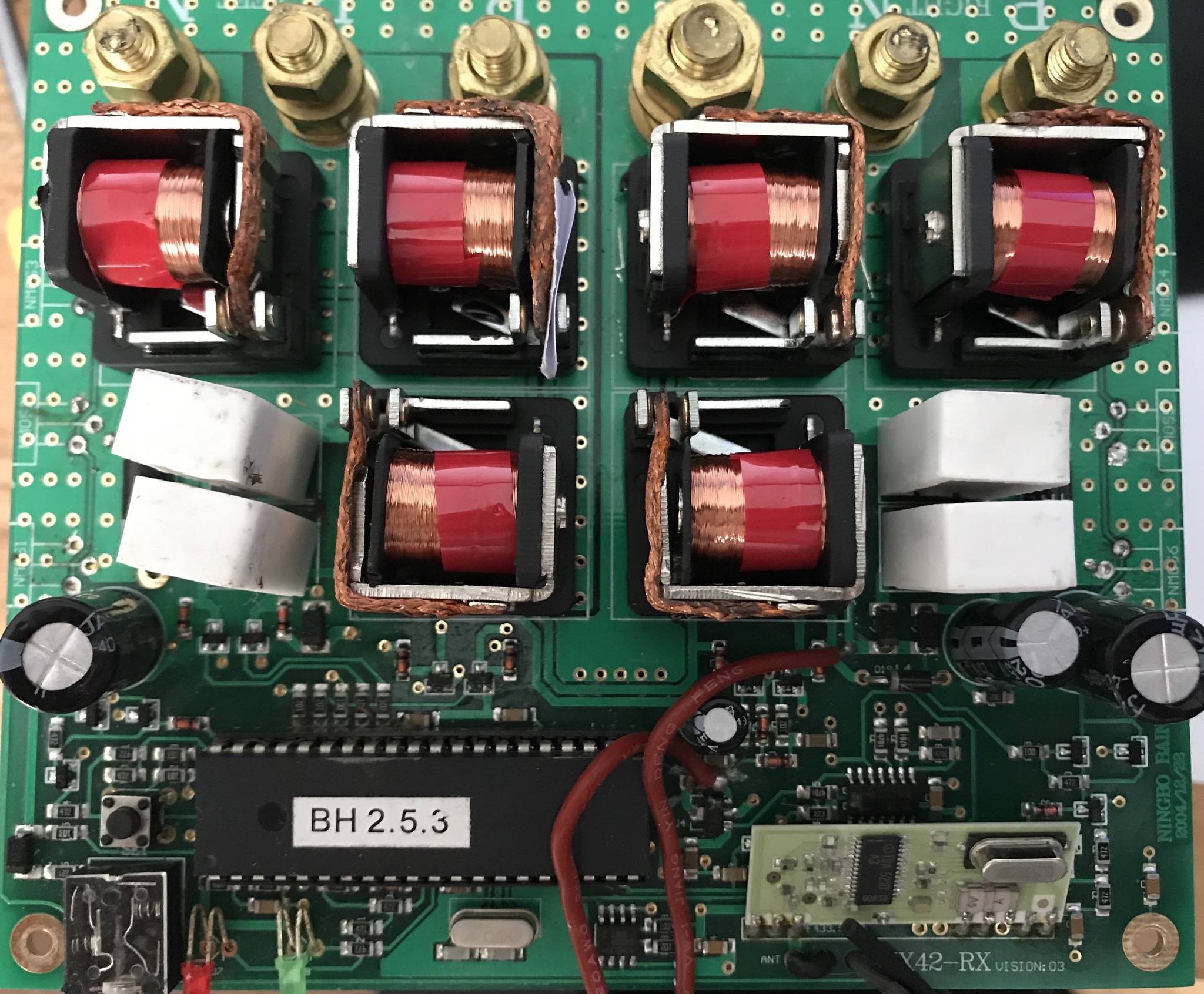
So I've photographed the two relevant halves of the board. You can see one of the FETs in the top right (NMOS6) and that's the broken side - so the thin track that leads under each cap is the gate line:

On the left side the gates are at 12v (red overlay) when the board is powered, on the right they're at 0v (blue overlay). Working vertically down the picture there are a pair of transistors - one's a J3Y and the other is really hard to ID - seems to have 3K written on it on the left, seems to have a hole in it on the right. I believe (if I'm understanding the datasheet schematic correctly) that this means the gates are connected to the emitters and on the working side the base pins are at 0v (blue), on the broken side the base pins are at 0.8v (orange). Everything else seems consistent each side of the board, though the layout differs the circuit seems to be the same. I stopped tracing back when I reached the same 5v (purple) or 12v (everythere else) so the majot difference seems to be this track that links all 3 transistors in some way - 0.8v on the broken side and 0v on the working
I drew this:

which I think is right, though the circuit simulator doesn't seem to indicate any 12v should reach the gates so it's probably incomplete, or I've got the BCEs the wrong way round, or something else to do with the transistors...
Any assist on that I should be doing to repair this?
Replacing the exploded transistor is first up, but can I raid any transistors out of a computer PSU i have kicking round? Or should I just be ordering exact replacements.. and what is the exact replacement for the one with the hole in?
Will the J3Ys need replacing too or might the voltages I see be explained by damage on only the one with the hole in?
Am I right in thinking these transistors are J3Y (easy to see) and a 3K (?) (It's a BC858B?) The transistor with the hole in has "3(hole)2" and the 2 is rotated 90 degrees. The "same" one on the working side of the board has "3KDO" written on it, except the DO is 90 degrees rotated and looks more like |)() because the letters have a break in the font at the top and bottom..
It's a bit nasty too, but if I don't get any joy from fixing this side, sould severing the gates line and bridging it to the gate line on other side of the board also work?
Thanks in advance for any pointers!
So, that part seemed ok.. The relays are fine, but there was no negative to the motors even tho the positive was OK
Turned out there were a parallel pair of MOSFETs on the negative side of things for each motor and all the MOSFETs were blown/gave crazy readings. I swapped them out like for like and one channel now works fine, the other channel has an issue:
It works fine if I use my multimeter to supply a bit of voltage to the MOSFET gates, but the board itself doesn't supply it. Having caught a comment on the web that "blown MOSFETs can cause the driver circuits to be damaged too" I'm checking the circuit that drives them. Because the board is more or less symmetrical in terms of components I traced back from the gates on each side to see where voltage differed, comparing working vs broken, and where it was the same. I'm no electronics genius, but it's proving to be an interesting learn
So I've photographed the two relevant halves of the board. You can see one of the FETs in the top right (NMOS6) and that's the broken side - so the thin track that leads under each cap is the gate line:
On the left side the gates are at 12v (red overlay) when the board is powered, on the right they're at 0v (blue overlay). Working vertically down the picture there are a pair of transistors - one's a J3Y and the other is really hard to ID - seems to have 3K written on it on the left, seems to have a hole in it on the right. I believe (if I'm understanding the datasheet schematic correctly) that this means the gates are connected to the emitters and on the working side the base pins are at 0v (blue), on the broken side the base pins are at 0.8v (orange). Everything else seems consistent each side of the board, though the layout differs the circuit seems to be the same. I stopped tracing back when I reached the same 5v (purple) or 12v (everythere else) so the majot difference seems to be this track that links all 3 transistors in some way - 0.8v on the broken side and 0v on the working
I drew this:
which I think is right, though the circuit simulator doesn't seem to indicate any 12v should reach the gates so it's probably incomplete, or I've got the BCEs the wrong way round, or something else to do with the transistors...
Any assist on that I should be doing to repair this?
Replacing the exploded transistor is first up, but can I raid any transistors out of a computer PSU i have kicking round? Or should I just be ordering exact replacements.. and what is the exact replacement for the one with the hole in?
Will the J3Ys need replacing too or might the voltages I see be explained by damage on only the one with the hole in?
Am I right in thinking these transistors are J3Y (easy to see) and a 3K (?) (It's a BC858B?) The transistor with the hole in has "3(hole)2" and the 2 is rotated 90 degrees. The "same" one on the working side of the board has "3KDO" written on it, except the DO is 90 degrees rotated and looks more like |)() because the letters have a break in the font at the top and bottom..
It's a bit nasty too, but if I don't get any joy from fixing this side, sould severing the gates line and bridging it to the gate line on other side of the board also work?
Thanks in advance for any pointers!

Comment