Next motherboards on the list: ASUS A8V-MX and MSI MS-7184. I got the two from the same seller on eBay. They were listed as “For Parts or Repair”, and seller even noted that one of the motherboards had bad caps (which the ASUS did… more on that in a bit). I wasn't expecting working boards, though, as there were no visible bad caps on the eBay pictures. But the ASUS turned out to work fine and had only one bad cap.
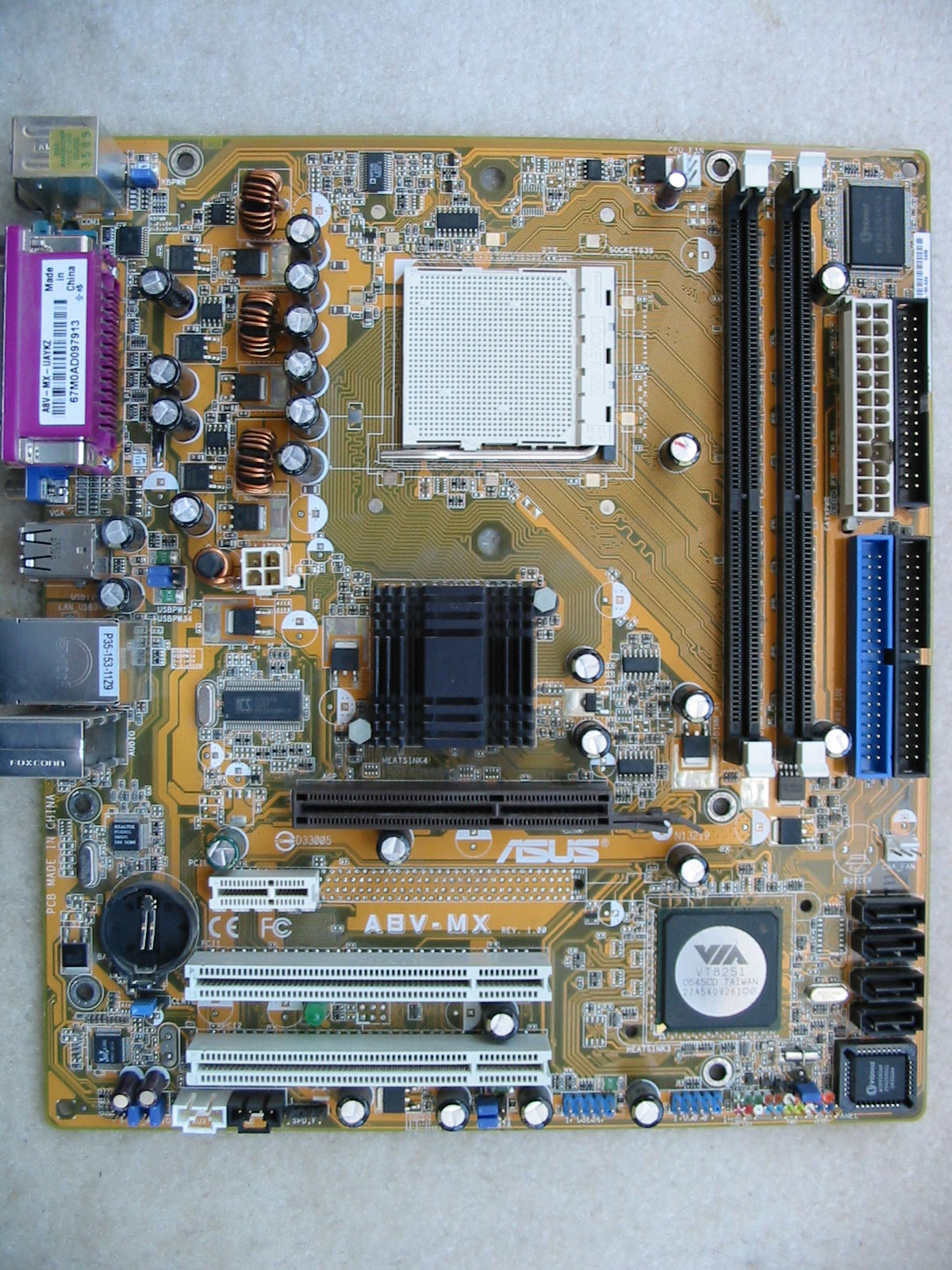
Some pictures of the ASUS A8V-MX motherboard as it came to me:
https://www.badcaps.net/forum/attach...1&d=1499309592
https://www.badcaps.net/forum/attach...1&d=1499309592
https://www.badcaps.net/forum/attach...1&d=1499309592
https://www.badcaps.net/forum/attach...1&d=1499309592
https://www.badcaps.net/forum/attach...1&d=1499309592
As seen in the images above, this motherboard uses mostly Panasonic FJ caps. For some reason, however, one of them was just slightly bulged (image 2). I don't remember if I ever tested that cap on my ESR meter or not. But other than that bulged cap, the rest were fine and the motherboard was actually working fine.
I replaced the single bulged Panasonic FJ 6.3 V, 820 uF cap with a Nichicon HZ 6.3V, 2200 uF cap (10 mm diameter cap from an Xbox 360 motherboard). One might question this choice, as I more than doubled the capacitance. But it turns out the free cap spot above that cap is in parallel with it. So most likely, the original design of this motherboard had way more capacitors than what is seen in the pictures. Thus, doubling the capacitance could not have hurt anything (and it didn't ).
).
This is the primary reason why I made cap diagram / cap map: I thought about filling in the missing cap spots at some point in time. So here is the cap diagram:
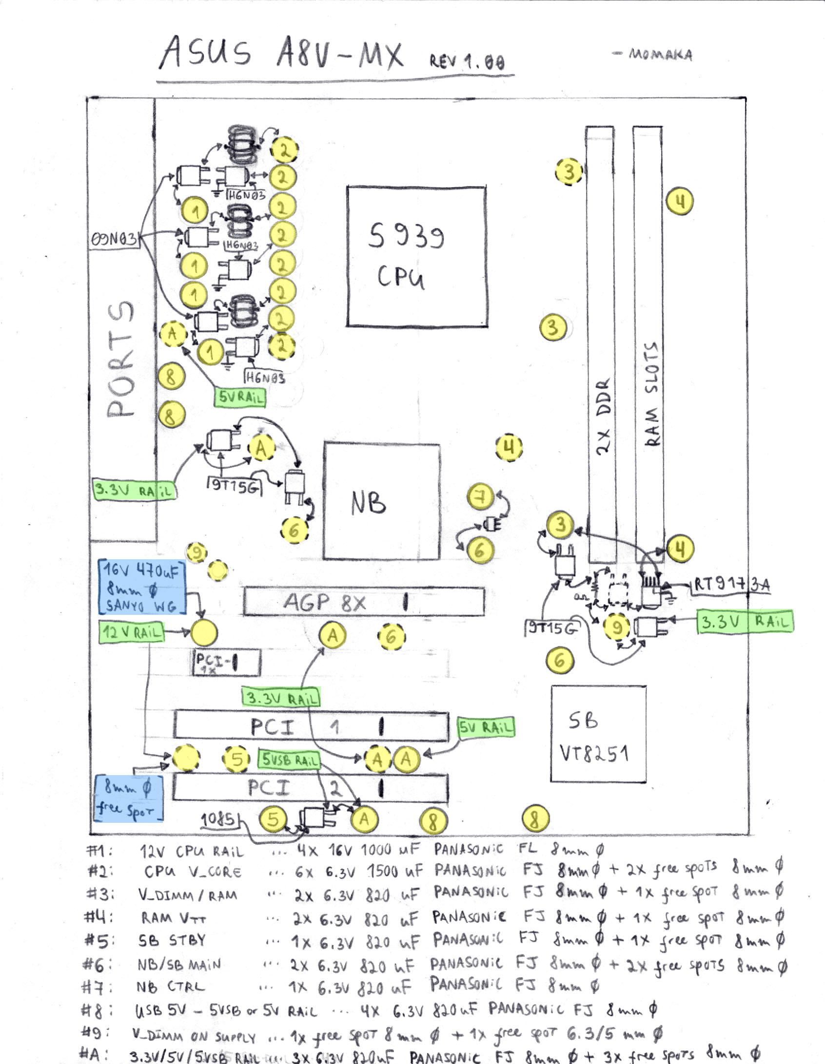
Normally, I go through all of the various voltage rails in detail. But since I did not really do any kind of serious recapping work here, I will go over only some of these, and much more briefly.
#1 and #2 are (as always on my cap diagrams) the CPU input and output sides, with the input being 12V and the output being around 1.4V (i.e. CPU V_core), or whatever the CPU uses for its core voltage. Worth noting is that this is *the only* buck-regulated rail on the motherboard. Everything else is linear-land. So when recapping this board (should you have anything different than Panasonic caps, like Chemicon KZG, for example), make sure to use good quality ultra-low ESR caps for #1 and #2. The rest of the rails don't need ultra-low ESR caps. Just regular low-ESR like Chemicon KY/KZE, Rubycon ZL, and Panasonic FR/FM should be good enough.
#3 and #4 are the RAM V_dimm and Vtt voltages, respectively (2.6V and 1.3V). The bulged cap was connected to a spot for #3.
#5 is the 3.3V Standby rail, generated from 5VSB by the 1085 regulator below the bottom PCI slot. (Not sure why I labeled it as “SB STBY”, as I don't think the Southbridge is powered in Standby/Soft-OFF mode. Only the LPC Super IO should be.)
#6 seems to be the Northbridge and Southbridge Vcc, 1.65 Volts.
#7 is actually the CPU Vtt / CPU<->NB HTT link voltage. Not sure why I labeled it “NB CTRL”. It is 1.3 Volts.
#8: USB ports… don't think I need to explain that.
#9 appears to be some kind of a rail that was never implemented. It might have been part of a multi-step linear regulator, to spread out the heat from the regulation more evenly. After all, it was typical for some ASUS motherboards from this era to have very hot-running regulators. This motherboard, however, does NOT have any. So that's probably why the cap and MOSFET for #9 were left out. Thus, no need to fill up spot #9.
#A: More filter caps for the various 3.3V and 5V rails on the board.
Unfortunately, I never bothered to fill in those empty cap spots either. Instead, I shoved the motherboard into a spare PC case (back when I actually had more spare PC cases than motherboards, lol ) and built a PC for random hardware testing / experimentation.
Worth noting is that this motherboard has both an AGP and a PCI-E 1x slot. And what's even more interesting is that the motherboard has a silkscreen (and the holes) for a full PCI-E 16x slot. So, I've always wondered what would happen if I actually installed a PCI-E 16x slot. Would the motherboard be able to take both AGP and PCI-E video cards? At the same time?
This intrigued me, so I decided to do some testing. But rather than pulling the PCI-E 1x slot and installing a 16x one (which frankly I think is quite a bit of work and probably too much effort for negligible gains, if any), instead I cut the end of the 1x slot, so it could take a full 16x video card. Because PCI-E is adaptive in nature, the video card should just run in 1x mode instead of 16x. – And it did!
However, here is the twist: in the BIOS, this motherboard only has the option to use AGP, PCI, or onboard IGP as the first monitor output – no option for PCI-E. As such, adding a PCI-E GPU in the 1x slot will show no output on the monitor until after the OS loads and one specifically sets that GPU to output to a monitor. That said, I was able to configure Windows (XP) to have my test PCI-E GPU (Radeon HD 2400) as the primary and sole monitor output in the system. The only small snag is that when the PC is first turned ON, the monitor remains OFF and nothing appears on it until the OS loads. So if one wants to go into BIOS and change some settings, the monitor will need to be connected either to the onboard IGP or an AGP video card for that. And then when the OS loads, the IGP/AGP video will go out and only the PCI-E one will be active. So accessing the BIOS does require some cable plugging and unplugging. But that's only if the PCI-E video card is used for output. It is also possible to use an AGP video card for one or two monitor outputs, and then the PCI-E for another one or two monitors. Thus, this motherboard is actually not bad in that regard.
The other notable thing is that this motherboard does have an option to change the Base/Host Clock. However, doing any kind of CPU over-clocking in this way (which is actually how it's done with socket 939 AMDs) makes the motherboard completely hang on POST. And the only way to fix the hanging is to remove the CMOS battery and reset CMOS. This happens even when the RAM is set to run at a slower clock and the HT link is set to a lower multiplier. I even tried setting the PCI-E clock to a “Fixed” frequency (there is an option for that as well). But still, the motherboard refuses to over-clock the CPU even by a single MHz.
Thus, this is clearly not a good motherboard for over-clocking. However, it is perfectly stable at the stock clocks. So if one needs a simple basic socket 939 motherboard that works, this one fits the bill. It has AGP and PCI-E 1x (which can be opened to take 16x cards), so it is possible to have a mutli-monitor setup. Also, ASUS actually did a good job with the CPU fan control, as the CPU fan can be set to run at a slow and reasonably quiet speed when idle. Once a pre-set temperature is exceeded in the BIOS, that's when the CPU fan can kick in harder (it's user-adjustable, which is really nice to see on an old basic board like this). This is something that many 939 motherboards from other manufacturers lack (that is, unless you bought a high-end gaming board or similar).
So all in all, it's a good motherboard.
Some pictures of the ASUS A8V-MX motherboard as it came to me:
https://www.badcaps.net/forum/attach...1&d=1499309592
https://www.badcaps.net/forum/attach...1&d=1499309592
https://www.badcaps.net/forum/attach...1&d=1499309592
https://www.badcaps.net/forum/attach...1&d=1499309592
https://www.badcaps.net/forum/attach...1&d=1499309592
As seen in the images above, this motherboard uses mostly Panasonic FJ caps. For some reason, however, one of them was just slightly bulged (image 2). I don't remember if I ever tested that cap on my ESR meter or not. But other than that bulged cap, the rest were fine and the motherboard was actually working fine.
I replaced the single bulged Panasonic FJ 6.3 V, 820 uF cap with a Nichicon HZ 6.3V, 2200 uF cap (10 mm diameter cap from an Xbox 360 motherboard). One might question this choice, as I more than doubled the capacitance. But it turns out the free cap spot above that cap is in parallel with it. So most likely, the original design of this motherboard had way more capacitors than what is seen in the pictures. Thus, doubling the capacitance could not have hurt anything (and it didn't
).This is the primary reason why I made cap diagram / cap map: I thought about filling in the missing cap spots at some point in time. So here is the cap diagram:
Normally, I go through all of the various voltage rails in detail. But since I did not really do any kind of serious recapping work here, I will go over only some of these, and much more briefly.
#1 and #2 are (as always on my cap diagrams) the CPU input and output sides, with the input being 12V and the output being around 1.4V (i.e. CPU V_core), or whatever the CPU uses for its core voltage. Worth noting is that this is *the only* buck-regulated rail on the motherboard. Everything else is linear-land. So when recapping this board (should you have anything different than Panasonic caps, like Chemicon KZG, for example), make sure to use good quality ultra-low ESR caps for #1 and #2. The rest of the rails don't need ultra-low ESR caps. Just regular low-ESR like Chemicon KY/KZE, Rubycon ZL, and Panasonic FR/FM should be good enough.
#3 and #4 are the RAM V_dimm and Vtt voltages, respectively (2.6V and 1.3V). The bulged cap was connected to a spot for #3.
#5 is the 3.3V Standby rail, generated from 5VSB by the 1085 regulator below the bottom PCI slot. (Not sure why I labeled it as “SB STBY”, as I don't think the Southbridge is powered in Standby/Soft-OFF mode. Only the LPC Super IO should be.)
#6 seems to be the Northbridge and Southbridge Vcc, 1.65 Volts.
#7 is actually the CPU Vtt / CPU<->NB HTT link voltage. Not sure why I labeled it “NB CTRL”. It is 1.3 Volts.
#8: USB ports… don't think I need to explain that.
#9 appears to be some kind of a rail that was never implemented. It might have been part of a multi-step linear regulator, to spread out the heat from the regulation more evenly. After all, it was typical for some ASUS motherboards from this era to have very hot-running regulators. This motherboard, however, does NOT have any. So that's probably why the cap and MOSFET for #9 were left out. Thus, no need to fill up spot #9.
#A: More filter caps for the various 3.3V and 5V rails on the board.
Unfortunately, I never bothered to fill in those empty cap spots either. Instead, I shoved the motherboard into a spare PC case (back when I actually had more spare PC cases than motherboards, lol
) and built a PC for random hardware testing / experimentation.Worth noting is that this motherboard has both an AGP and a PCI-E 1x slot. And what's even more interesting is that the motherboard has a silkscreen (and the holes) for a full PCI-E 16x slot. So, I've always wondered what would happen if I actually installed a PCI-E 16x slot. Would the motherboard be able to take both AGP and PCI-E video cards? At the same time?
This intrigued me, so I decided to do some testing. But rather than pulling the PCI-E 1x slot and installing a 16x one (which frankly I think is quite a bit of work and probably too much effort for negligible gains, if any), instead I cut the end of the 1x slot, so it could take a full 16x video card. Because PCI-E is adaptive in nature, the video card should just run in 1x mode instead of 16x. – And it did!
However, here is the twist: in the BIOS, this motherboard only has the option to use AGP, PCI, or onboard IGP as the first monitor output – no option for PCI-E. As such, adding a PCI-E GPU in the 1x slot will show no output on the monitor until after the OS loads and one specifically sets that GPU to output to a monitor. That said, I was able to configure Windows (XP) to have my test PCI-E GPU (Radeon HD 2400) as the primary and sole monitor output in the system. The only small snag is that when the PC is first turned ON, the monitor remains OFF and nothing appears on it until the OS loads. So if one wants to go into BIOS and change some settings, the monitor will need to be connected either to the onboard IGP or an AGP video card for that. And then when the OS loads, the IGP/AGP video will go out and only the PCI-E one will be active. So accessing the BIOS does require some cable plugging and unplugging. But that's only if the PCI-E video card is used for output. It is also possible to use an AGP video card for one or two monitor outputs, and then the PCI-E for another one or two monitors. Thus, this motherboard is actually not bad in that regard.
The other notable thing is that this motherboard does have an option to change the Base/Host Clock. However, doing any kind of CPU over-clocking in this way (which is actually how it's done with socket 939 AMDs) makes the motherboard completely hang on POST. And the only way to fix the hanging is to remove the CMOS battery and reset CMOS. This happens even when the RAM is set to run at a slower clock and the HT link is set to a lower multiplier. I even tried setting the PCI-E clock to a “Fixed” frequency (there is an option for that as well). But still, the motherboard refuses to over-clock the CPU even by a single MHz.
Thus, this is clearly not a good motherboard for over-clocking. However, it is perfectly stable at the stock clocks. So if one needs a simple basic socket 939 motherboard that works, this one fits the bill. It has AGP and PCI-E 1x (which can be opened to take 16x cards), so it is possible to have a mutli-monitor setup. Also, ASUS actually did a good job with the CPU fan control, as the CPU fan can be set to run at a slow and reasonably quiet speed when idle. Once a pre-set temperature is exceeded in the BIOS, that's when the CPU fan can kick in harder (it's user-adjustable, which is really nice to see on an old basic board like this). This is something that many 939 motherboards from other manufacturers lack (that is, unless you bought a high-end gaming board or similar).
So all in all, it's a good motherboard.
Attached Files
if you find these attachements useful please consider making a small donation to the site


 ), I think early 2006 datecodes are visible on the HZ and HN if you look very carefully. The issue may be that the oxidizers in the electrolyte are not always 100% successful in absorbing excessive hydrogen or precluding water-driven corrosion, which is why some may arbitrarily bloat a la KZG and KZJ.
 Perhaps my memory is faltering on me, but I recall you said five years ago that one of the 1500uF 16V MCZ you reverse polarized had formed permanent gas inside - IE, it was hard as a rock and you couldn't push the top back down.
 ). And given that the Xbox 360 board above comes without anything else, I think we can be certain that some idiot already tried to reflow these and failed.


Comment